Today, we’re excited to share our Summer Update to Flux AI Auto‑Layout, a collection of improvements designed to make one‑click PCB routing more reliable, transparent, and adaptable to your real‑world workflows.
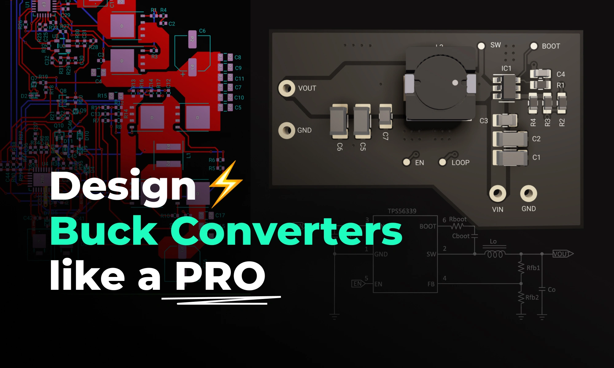
Design high-performance buck converters with proven PCB layout best practices. Cut noise, save space, and optimize your power supply design with this guide.
At its heart, a buck converter is nothing more than three core elements working together to regulate a higher voltage to a lower voltage—and understanding these will make everything else click.
Here’s the simple math for a 12 V→5 V converter:

That 42 % duty cycle tells the MOSFET exactly how long to stay on each cycle so the LC filter averages out to 5 V.
Behind the scenes, a control IC monitors the output, compares it to an internal reference, and tweaks that duty cycle in real time to handle changing loads or input swings. But regardless of controller complexity, the switch + inductor + filter always remain the converter’s heart and soul.
Pick the wrong inductor, and you may face problems like overheating, excessive output ripple, or even core saturation that starves your load under sudden demand. To help you choose wisely, here’s what every beginner EE should know about inductor characteristics:
Pro tip: Choosing an inductor with a bit of extra saturation current rating and modestly lower DCR gives you valuable headroom during prototyping—preventing unexpected heat and ripple issues as your load conditions change.
A combination of MLCCs and a bulk cap covers ripple from kHz to MHz—get this wrong, and you’ll hear audible squeals or see output spikes.
Deep dive: MLCCs lose capacitance under DC bias and heat. And yes, they can sing! Ensure parallel MLCCs are carefully secured mechanically to mute piezo effects. Placing smaller-value capacitors first help to attenuate the high frequency singing in the larger smoothing caps.
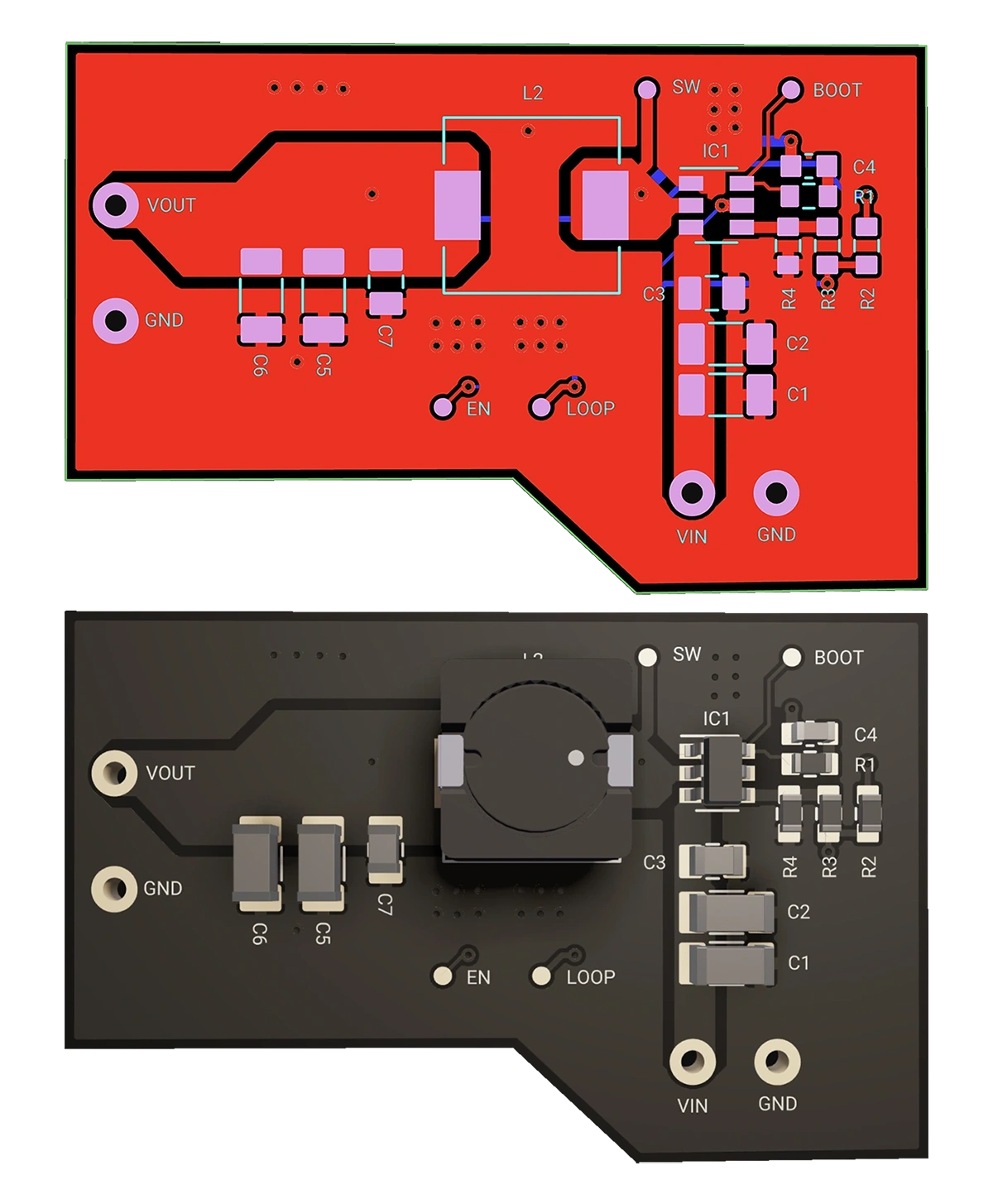
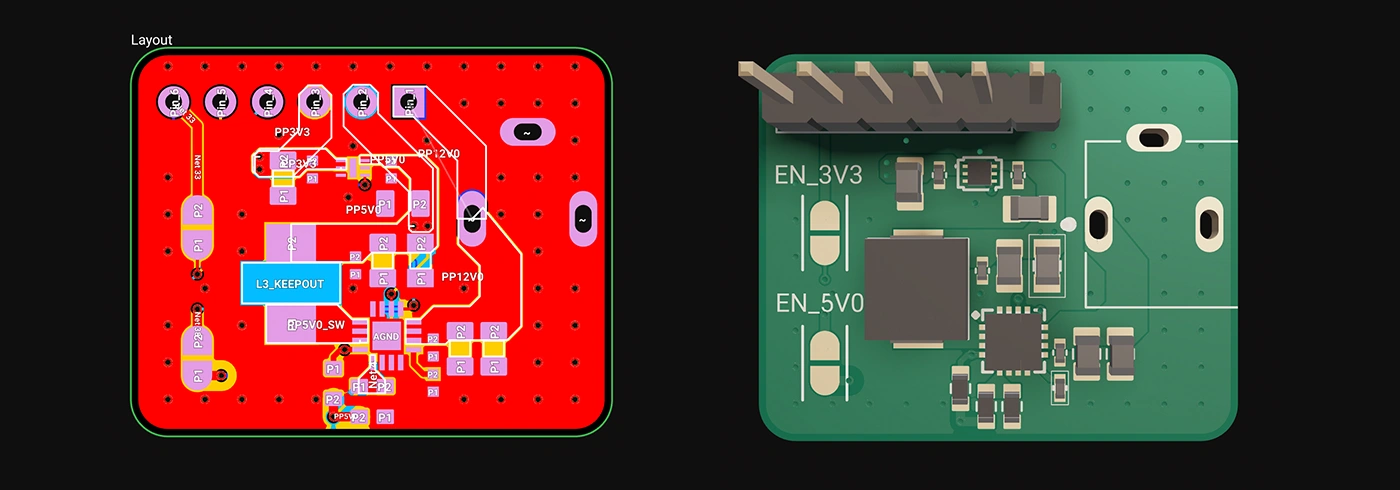
Having chosen your parts, layout is your next battleground. The difference between a noisy, inefficient converter and a clean, reliable one often comes down to copper placement. Follow these steps to keep that switching loop tight and your ground plane unbroken.
Remember: “Keep the switching loop tiny and the ground plane continuous.”
Minimize the Switch Loop
Separate Control Signals
From full DIY assemblies to one-click, ready-to-use modules, these different topologies trade off flexibility, board space, and time-to-market. Pick the one that fits your project rhythm.
Each template already includes polygon pours for power and ground, and via-stitching. Once cloned, customize only what matters.
Ground planes are a default in any Flux project, which reflows around all parts and pads to help with noise isolation. Polygons are now in Flux helping you leverage wide current paths for your output voltage to flow through. Adjust thermal reliefs, keep-outs, and copper weights without redrawing anything.
🤖 Copilot: Your AI EE Mentor:
Stuck on compensation loops or gate-resistor values? Ask Copilot right inside the editor. It explains theory, suggests values, and even pulls tables from datasheet PDFs.
🛣️ Auto-Layout for Non-Critical Nets:
Zone off low-speed signals—UART, I²C, sensors—and let Auto-Layout handle them. That frees you to hand-route the critical buck loops that define performance.
“Copilot help me determine the best orientation of U1 to minimize the switching current loop.”
Think of this as your design checklist: tape it to your monitor, keep it next to your keyboard, or fold it in your notebook. Pull it up whenever you need a formula, a layout reminder, or a topology refresher.
With Flux’s polygons, AI Copilot, and Auto-Layout, you’ll spend less time wrestling nets and more time optimizing your power stage—so you can ship faster and with confidence.
👉 Get started now » Open Flux and Clone a Buck Converter
Now, Flux Copilot can learn how you work—your design principles, part selection preferences, schematic style guidelines, and testing workflows—and remember them automatically.
That’s why we built Copilot Knowledge: a way to offload your internal mental graph into something persistent, reliable, and AI-accessible. Now, Flux Copilot can learn how you work—your design principles, part selection preferences, schematic, and testing workflows—and remember them automatically.
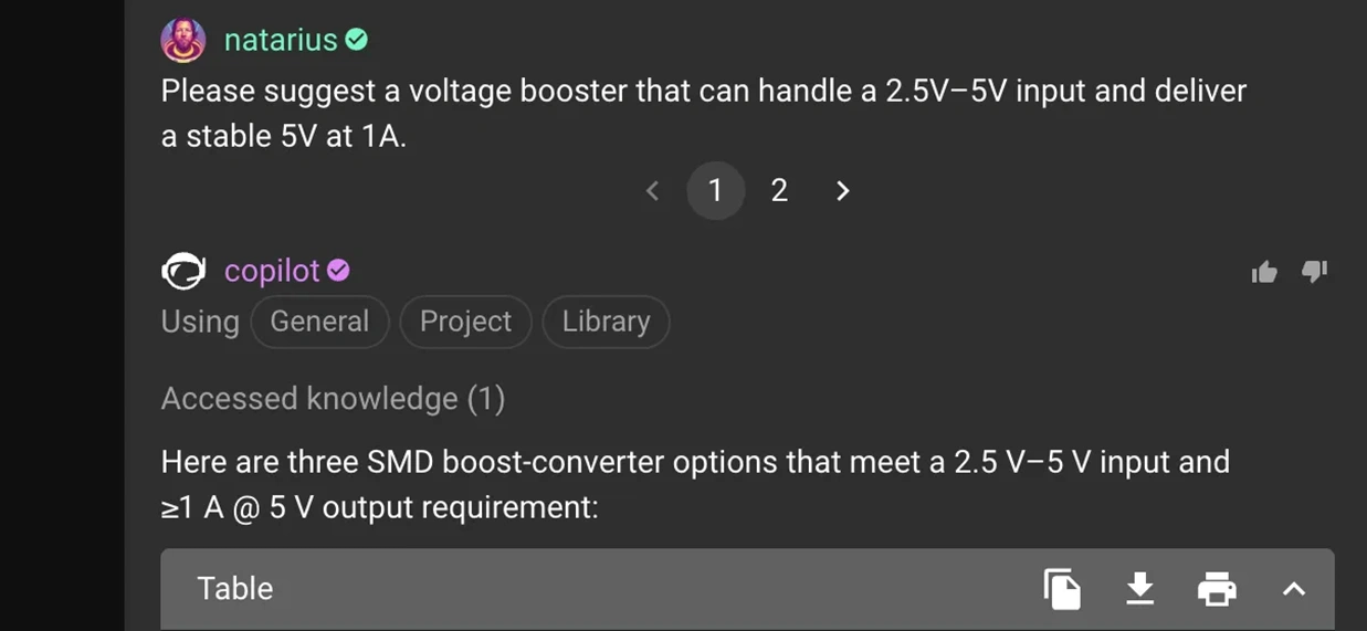
It’s like onboarding a new teammate who can understand and distill your process, catches inconsistencies, and applies the right context when you both need it. But this isn’t just memory—it’s leverage. Copilot uses its knowledge to improve its suggestions and take smarter actions helping you move faster with fewer mistakes.
And the best part? You don’t have to change the way you work. Just talk to Copilot as you normally would. When it detects a relevant insight, it’ll ask if you want to save it. Approve what matters, and your personal or project-level Knowledge base builds naturally over time. Let’s dive in!
Knowledge is persistent memory for your Copilot. It stores reusable instructions, tribal knowledge, and workflow guidance that help Copilot work more like you do.
You can teach Copilot anything that improves its judgment across tasks:
This means Copilot can tailor its help based on your intent and context—not just the immediate task at hand.
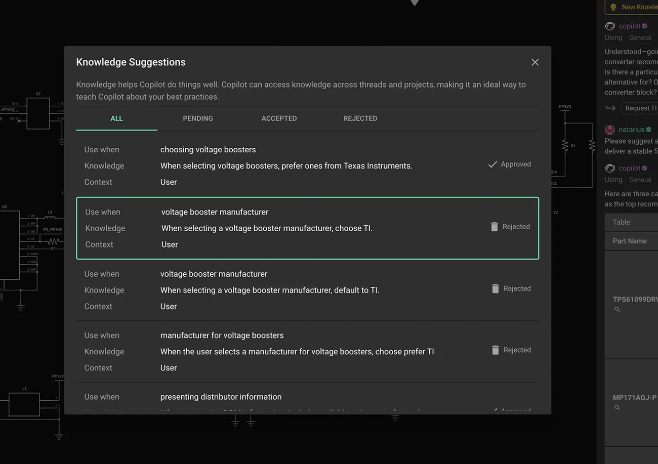
As you chat with Copilot, it now looks for teachable moments. If you say something like:
“Always use TI parts for voltage boosters” or
“Start every layout with DRC checks”
Copilot will offer to turn that insight into a reusable Knowledge entry.
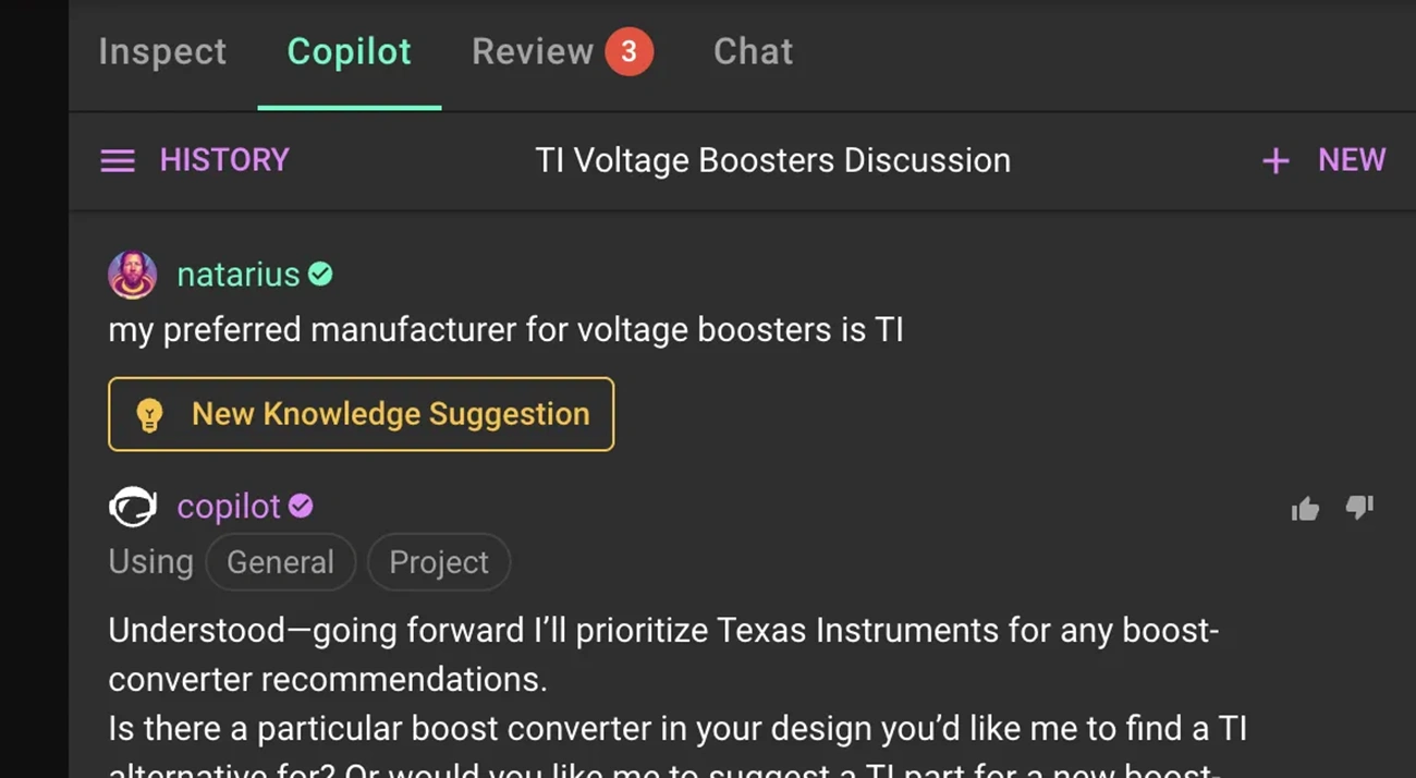
You can accept, reject, or refine it. Once accepted, it becomes part of Copilot’s working memory. And the next time you’re designing a similar circuit, it’ll know to apply that guidance without being asked.
You can also manually add entries from your profile or project settings. Every Knowledge entry you create makes Copilot smarter and more aligned with how you think.
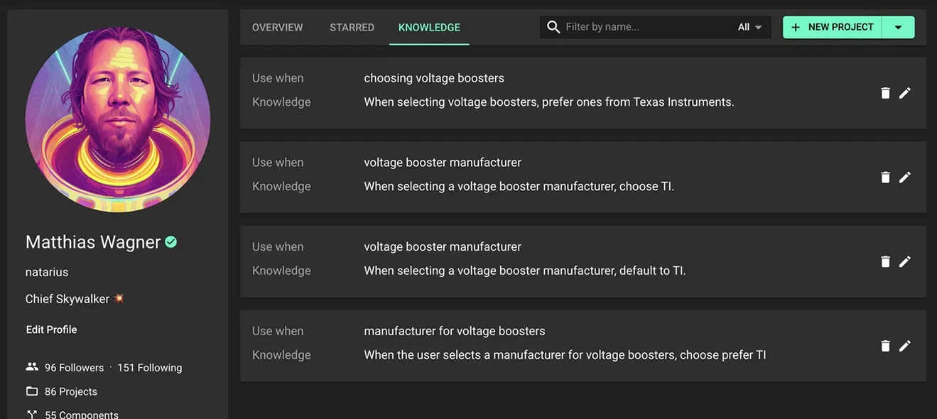
Every time you save a piece of Knowledge, you can decide where it should apply: just to this project, or to everything you work on going forward.
If you choose project-level, Copilot will only use that Knowledge within the specific project it was saved in. This is ideal for capturing things like client-specific standards, board-specific constraints, or one-off decisions that aren’t relevant elsewhere.
If you choose user-level, Copilot will use that Knowledge across all your future designs. This is where you’ll save broader design habits—like how you label nets, the parts you tend to default to, or your general approach to testing.
Scoping Knowledge like this keeps Copilot flexible. It lets you define reusable standards when it makes sense and isolate exceptions when needed—just like you would when explaining something to a junior engineer stepping into a new design.
Getting the most out of Copilot Knowledge is a lot like onboarding a new hire. The more context you give early on, the more independently—and accurately—they’ll be able to contribute.
When Copilot suggests saving a Knowledge entry, it's your opportunity to share something you’d normally explain to a colleague joining the project for the first time. That might be a naming convention you always use, a preferred component vendor, a filter that’s worked well in the past, or a key review step you never skip. These kinds of insights are rarely documented—but they’re essential to maintaining quality and consistency in real designs.
You don’t need to front-load everything. Knowledge builds naturally over time. But with just a little intentional input, Copilot becomes a design partner who doesn’t just follow your lead—it understands how you lead, and why.
Copilot Knowledge is available now, and there’s nothing new to learn to start using it. Just keep working the way you already do. As you chat with Copilot, it will surface patterns and insights you’ve taught it—then offer to save them as reusable Knowledge.
Start with something simple. A naming convention you always use. A go-to part family. A review checklist. Save that, and keep going. Over time, your Knowledge base grows with you—project by project, decision by decision—until Copilot starts feeling less like a tool and more like a teammate who’s been working with you for years.
This is how design becomes more scalable, more consistent, and more collaborative—without slowing you down.
{{open-flux-start-teaching-copilot}}
This guide is here to help. Based on the most common questions we hear from our users, it walks through practical solutions to unblock your designs and give you more confidence as you build.
Flux is built to help you move fast—from idea to fully routed board—with powerful automation, AI-assisted design, and intuitive tools that make professional workflows accessible to everyone. But even the best tools come with a learning curve, and occasionally you might run into something unexpected.
This guide is here to help. Based on the most common questions we hear from our users, it walks through practical solutions to unblock your designs and give you more confidence as you build.
Whether you’re new to PCB design or just new to Flux, these tips are designed to save you time and help you get the most out of the platform.
“Why am I seeing DRCs for overlapping copper?”
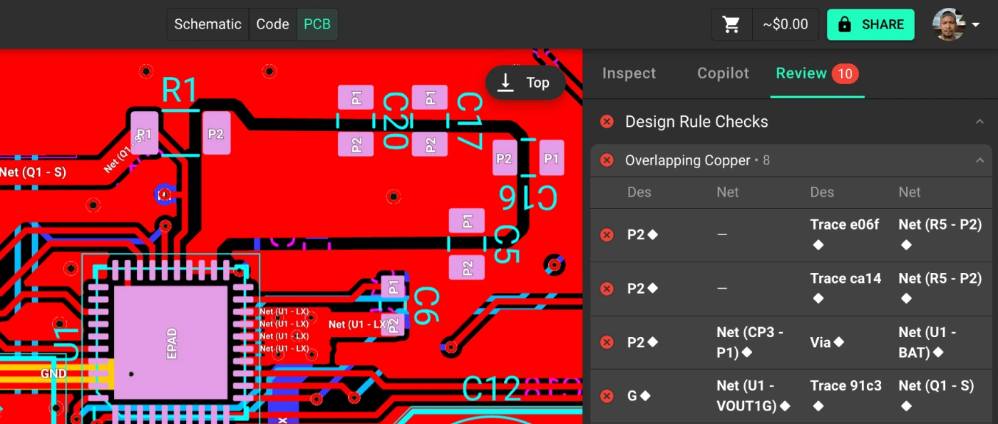
Overlapping copper errors typically occur when copper from two different nets occupies the same area on a PCB layer. This can lead to short circuits, unexpected connections, and compromised board performance. Flux flags these cases as design rule violations to protect the electrical integrity of your design.
Tip💡: Enable all layers in your visibility settings. Overlaps sometimes occur between nets on different layers and can be easy to miss.
“Why is Flux saying I have conflicting fills?”
Flux automatically adds GND fills to each layer, but if more than one net is assigned a fill on the same layer, it creates a conflict. The system prevents this to ensure clean and predictable copper behavior.
Only one net should apply fills per layer—typically GND, unless you're working on advanced designs requiring power planes or split fills.
“What is floating copper, and why is it an error?”
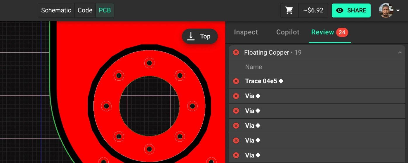
Floating copper refers to any copper (usually a fill or trace) that is no longer electrically connected to its assigned net. This often happens when components are moved or deleted, leaving behind orphaned copper.
Keeping copper grounded and connected ensures electrical correctness and helps avoid manufacturing issues down the line.
“My board has no visible GND fills—what’s wrong?”
By default, Flux adds ground fills to all PCB layers for the GND net. If you’re not seeing them, it’s usually a configuration or visibility issue rather than a bug.
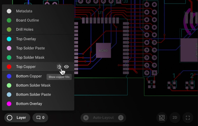
Fills play a crucial role in EMI reduction, return path continuity, and thermal performance, so it's important to verify they're in place.
“I created a part, but I can’t find it in my library—where is it?”
When you create a custom part in Flux, it lives in a separate project until you publish it. Publishing is what makes it available in your global or team library.
🔒 By default, newly created parts are private.
If you want others to use it, click “Share” and set visibility permissions. Just remember to re-publish after updating sharing settings.
“I imported my Altium file, but nothing shows up.”
This usually comes down to format. Flux only supports ASCII format when importing from Altium Designer. If you export in binary format, the import will silently fail or appear blank.
To verify: open the file in a text editor. If it’s human-readable, it’s ASCII. If it’s gibberish, it’s binary.
Large schematics? Try breaking them into modules for smoother imports.
“Why is Auto-Layout stuck on ‘Optimizing’?”
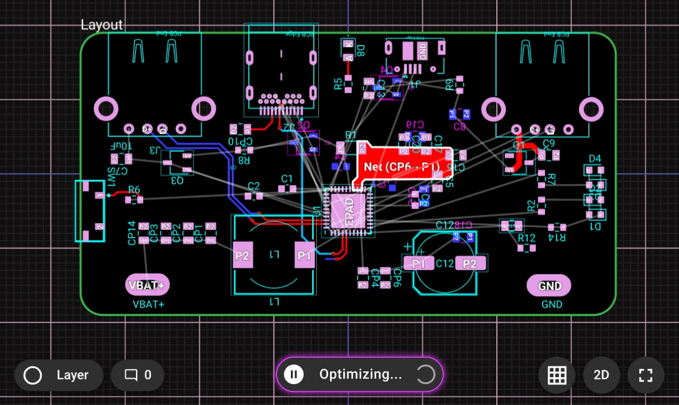
Flux’s Auto-Layout feature can take time—especially on complex boards. The “Working” state may appear stuck if DRCs are unresolved, or if the board has high routing complexity.
If needed, hit Stop to investigate and restart. Just be aware that stopping clears progress if changes haven’t been applied.
“I imported a KiCAD part—why is it incomplete?”
Flux supports KiCAD library imports, but some metadata—like footprints or 3D models—need to be linked manually.
Once set, the part will behave like any other in your library.
“Why is Copilot making strange connections?”
Flux Copilot is optimized for specific, context-aware actions. It’s not intended to auto-wire an entire schematic in one go, and complex instructions often reduce its accuracy.
With more focused prompts, Copilot becomes a powerful assistant rather than a source of confusion.
“Where can I go when I need support fast?”
We want you to feel confident using Flux, even when things aren’t going smoothly. Here's how to get help:
Building with Flux means working with one of the most forward-moving platforms in EDA—but we also know that speed comes with bumps along the way. This guide is here to help you smooth them out and keep shipping.
Most importantly, you’re not alone. Whether it’s a UI quirk, a Copilot misfire, or just needing a second pair of eyes, we’re here to help—through docs, videos, chat, or Slack.
And if something isn’t working the way you expect, let us know. The fastest way we improve Flux is with your feedback.
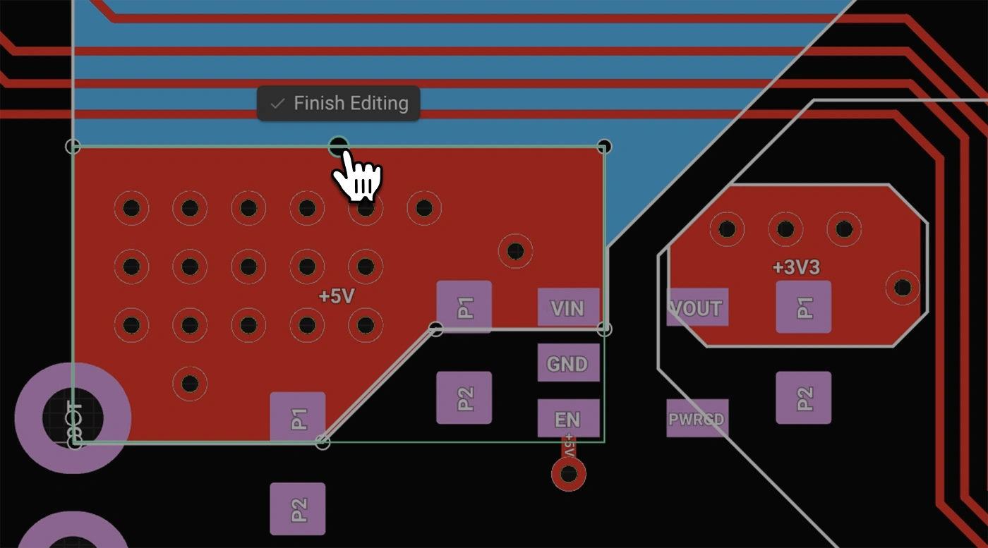
We're excited to unveil our Smart Polygon system in Flux! This powerful capability builds on top of our automatic copper fills to transform how you create and manage custom copper areas in your PCB designs.
Smart Polygons in Flux behave intuitively like traces, making them straightforward to learn and use—start directly from any pad with automatic net association, simply click to place and adjust points, and watch as copper intelligently reflows in real-time. Let’s dive in!
In PCB design, polygons are customizable copper shapes directly tied to a specific net. They’re crucial because they significantly influence the electrical performance and reliability of your PCB. Polygons allow you to optimize your board layout for specific electrical properties, including improved grounding, controlled impedance, and efficient heat distribution.
Specifically, polygons are indispensable for:
{{polygons-examples}}
Unlike zones—which define areas where copper cannot exist—polygons actively conduct electricity and shape your board's electrical performance, making them fundamental for advanced PCB designs.
At Flux, we prioritize intuitive, user-friendly workflows. Automatic copper fills were the first step. Now with polygons, we've continued this approach:
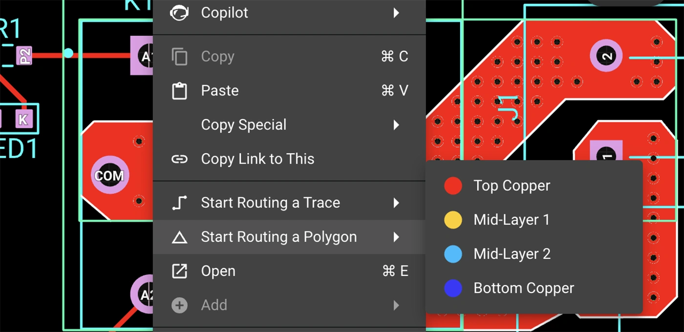
Polygons in Flux behave intuitively like traces, making them straightforward to learn and use, right from the start.
Polygons in Flux pack powerful functionality without complexity:
Polygons unlock new possibilities in your PCB designs. Here are a few practical ways you'll benefit:
Whether you're just dipping your toes into PCB design or you’re a veteran engineer tackling complex layouts, polygons in Flux offer the ideal balance of simplicity and capability:
Polygons are available now in Flux, ready to enhance your PCB design capabilities. Explore this powerful feature today and experience firsthand how advanced design can truly be this easy.
Dive in now and check out our detailed polygon documentation or jump straight into Flux to try it yourself. We can't wait to hear what you think!
In this post, we’ll explore why these concepts matter, how they impact signal integrity and power distribution, and what to keep in mind as you design. If you want to go deeper into implementation details—like when to use zones, where to place stitching vias, or how to avoid stack-up pitfalls—we’ve created a detailed PDF guide just for that.
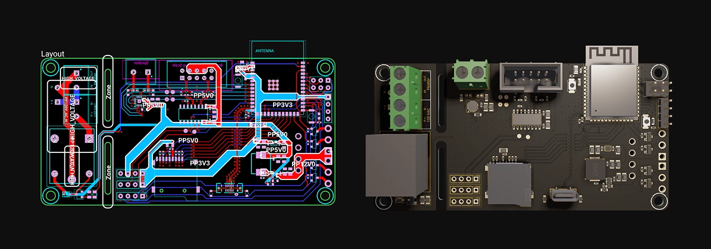
That’s where ground planes, zones, and stackup symmetry come in. They’re the quiet guardians of signal integrity, and Flux is built to help you get them right—without the guesswork.
In this post, we’ll explore why these concepts matter, how they impact signal integrity and power distribution, and what to keep in mind as you design. If you want to go deeper into implementation details—like when to use zones, where to place stitching vias, or how to avoid stackup pitfalls—we’ve created a detailed PDF guide just for that.
{{download-gnd-power-guide}}
Every signal you route is part of a circuit. And that circuit includes the return path—the signal that flows back to the source. At high speeds, this return doesn't just wander through your board—it seeks the lowest impedance path back.
That path is normally the ground plane directly beneath the signal layer. If the plane is continuous, the return path stays tight, inductance stays low, and EMI stays minimal.
But if the ground is broken—say, by a split—the return path will form a bigger loop. And bigger loops might mean bigger problems: signal distortion and radiated emissions that could cause a failed EMI test.
Good return paths are invisible when they work, and painfully visible when they don’t.
You’ve probably heard the advice: “Split your ground plane between analog and digital.” Sometimes that’s sound engineering. But often, it leads to more trouble than it solves.
The key question isn’t “Should I split my ground plane?”—it’s “Will this split create more noise than it prevents?”
In most cases, you should avoid splitting the ground plane. Here's why:
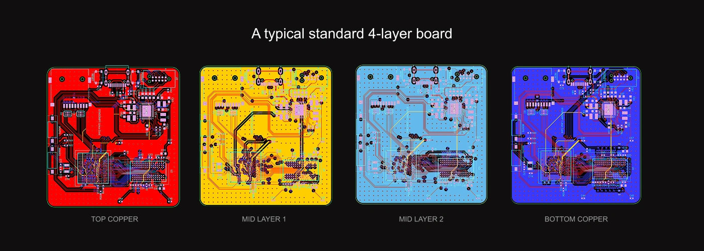
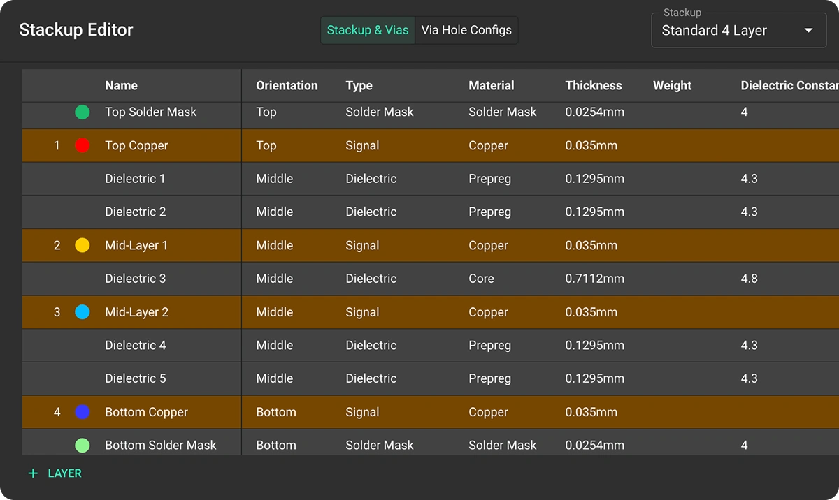
A PCB stackup isn’t just a layer count—it’s a design decision that affects everything from signal integrity to manufacturing yield.
When your layout starts pushing higher speeds or tighter constraints, your stackup becomes critical. It defines the electrical environment for your signals and the mechanical stability of your board.
For most standard boards—say, 4 to 6 layers on 1.6 mm FR4—mechanical issues like warpage are rarely a showstopper with modern fabrication processes. Today’s board houses are well-equipped to handle these with balanced copper and proper lamination.
But in more demanding cases, stack symmetry still matters:
The rule of thumb: the more complex or thermally sensitive your board, the more stack symmetry and copper balance matter. It’s not just about layout—it’s about ensuring the board survives fab, assembly, and real-world use.
If you remember nothing else, start with these rules:
We’ve built these rules into Flux—not as rigid constraints, but as default guardrails. So you can break them when needed—but only when you know you need to.
High-speed, low-noise boards don’t happen by accident. They’re designed intentionally—from the copper up. Whether you're debugging EMI issues or laying out a complex mixed-signal board, your ground strategy is the foundation.
With Flux, you don’t need to memorize every trick in the book. We’ve integrated the most important ones into your workflow—so you can focus on building, not second-guessing.
Ready to ground your designs the right way?→ Open Flux and give your next project the return path it deserves.→ Or dive deeper into Zones and Cutouts » | Stackup Editor »
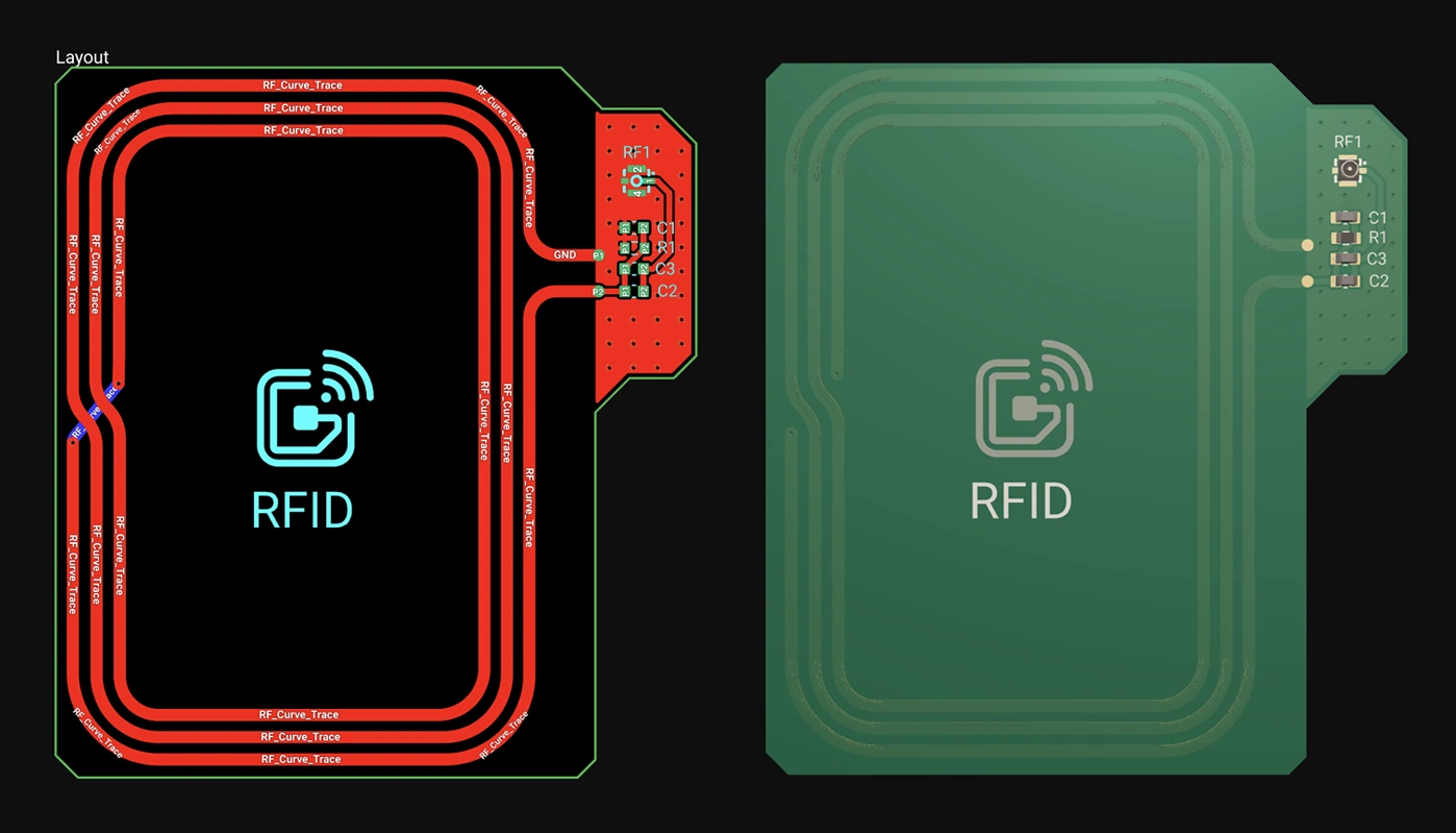
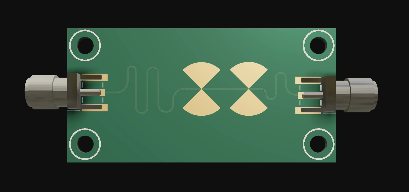
Whether you’re routing high-speed buses, fine-tuning antennas, or laying out clean RF filters, sharp 90º or even 45º angles can be a serious bottleneck. Now, you can create precisely curved elbows across entire nets—or dial them in trace by trace—with full control over radius, inheritance, and overrides.
We’re excited to announce one of the most requested features from advanced users: Curved Traces are now available in Flux!
Whether you’re routing high-speed buses, fine-tuning antennas, or laying out clean RF filters, sharp 90º or even 45º angles can be a serious bottleneck. Now, you can create precisely curved elbows across entire nets—or dial them in trace by trace—with full control over radius, inheritance, and overrides. Curved Traces were built to work the way you already do in Flux. You don’t need to micromanage every elbow—just set your rules once, and let the system handle the rest.
Need to override an elbow? You can. Want to apply curved traces to an entire layout? Go for it. You’re in the driver’s seat, and the system has your back with smart defaults, inheritance, and DRCs that surface only when needed.
This release sets the stage for what’s next: full support for flex and rigid-flex boards. Curved Traces are the first major unlock—and we’re actively building the rest. Flex is on the way.
This isn't just about cosmetics. Curved traces improve routing quality, unlock new design styles, and remove a major blocker for:
Until now, you had to work around Flux’s sharp elbows. Now, you can design the way the pros do—with full control over every bend.
Curved Traces give you a new level of control over how your signals move across the board—whether you’re designing critical paths or polishing the final layout. To use curved traces:
1. Enable curved routing - Set the Trace Shape rule to "Curve" at the layout, net, or individual segment level. This tells Flux to apply curves instead of sharp elbows wherever possible.
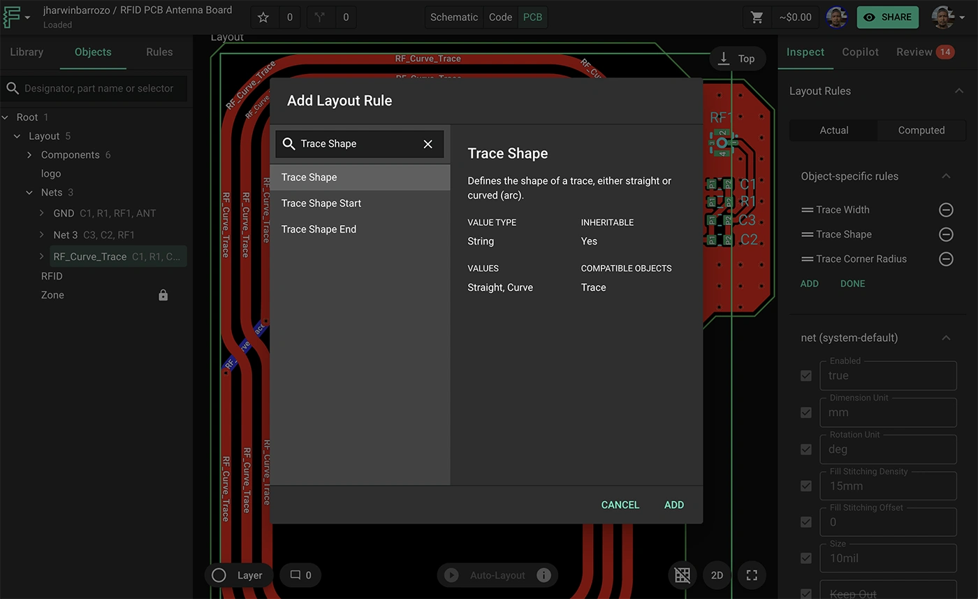
2. Set a minimum radius - Use the Trace Corner Radius Minimum rule to define the smallest allowable curve. This helps ensure manufacturability—especially for tight layouts or impedance-sensitive routes.
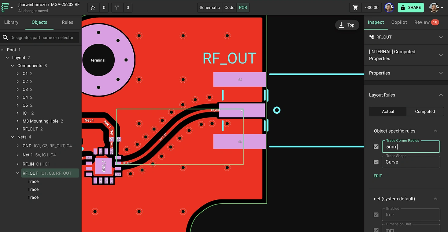
3. Leverage inheritance - Apply your rules at the layout or zone level so they cascade automatically. You can mark rules as !important to make them stick when conflicts arise.
4. Override specific elbows - Need more control? Just click and drag the trace elbow or use Trace Corner Radius Start/End or Trace Shape Start/End to adjust a specific corner without affecting the whole trace.
5. Watch for DRC warnings - Flux will flag any elbows that can’t meet your minimum radius—so you can adjust your layout before it becomes a real problem.
6. Mix manual + auto-routing - Route critical traces by hand to maintain control—then auto-route the rest. Flux will respect your curved segments and finish the job cleanly.
If you’ve ever spent time nudging elbows, adjusting angles, or finessing a meander by hand, this is the update you’ve been waiting for.
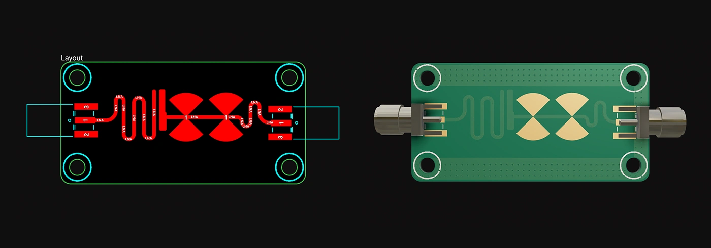
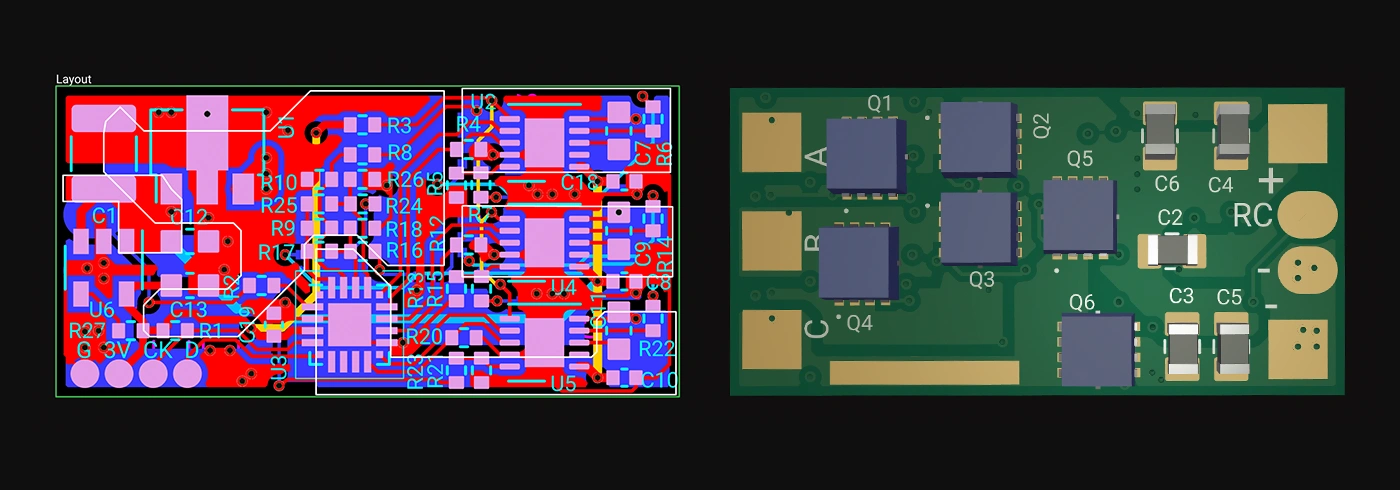
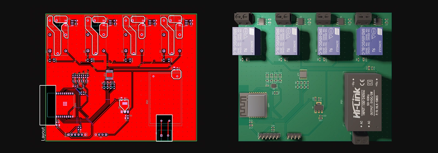
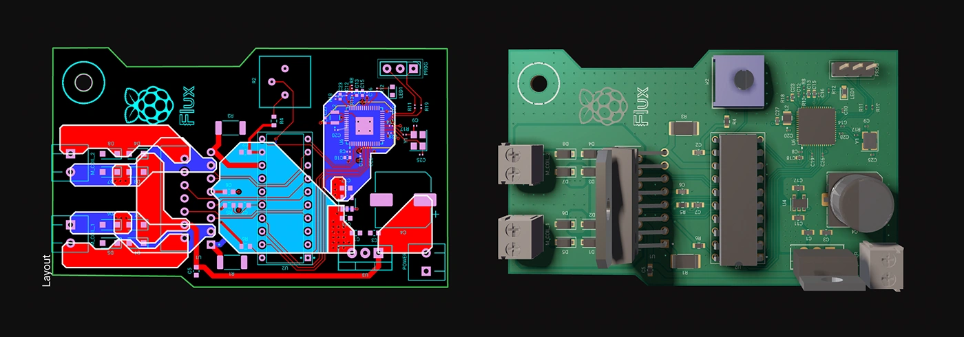
Want to see what’s possible? We’ve put together a few fully forkable example projects that showcase curved trace routing in the wild:
Open them, explore the layout rules, and make them your own.
Curved Traces are a foundational feature—especially for advanced workflows. But they’re also a signal: we’re investing deeply in professional-grade capabilities, from stackups and automatic impedance control to AI auto-layout and AI-assisted design reviews. If Flux wasn’t quite enough for your pro projects before, now’s the time to jump back in.
Curved Traces are available to all users starting today. Just open any project, apply the "Curve" trace shape in your layout rules, and start routing. It's that simple.
Got feedback or something cool to share? Post in the Flux community or tag us—we’d love to feature your work.
Let’s bend some traces.
👉 Open Flux and try it now.