July 31, 2025
AI Auto-Layout Just Got Smarter
Share
BuildWithFlux


This update is a set of pragmatic steps toward our vision of Auto‑Layout as your trusted routing assistant. Here's what's improved:
Auto‑Layout still works best when guided by thoughtful placement, clear net names, and rulesets—but now it’s a more predictable, collaborative partner in your design process.
Classify your nets into seven priority buckets—High Speed, Analog, Power, Medium Speed, Low Speed, Uncertain, and Ground—and Auto‑Layout will route them in that exact order. Flux will infer the Net Type of each net in your design, but you can check and change the inference by selecting a net and altering the Net Type property.
High‑speed nets go first.
Analog nets get their own quiet lanes.
Power nets find robust copper paths.
This helps ensure your most sensitive signals aren’t forced into awkward detours, delivering a draft layout that mirrors your own routing instincts.
Previous versions of Flux Auto‑Layout often scrunched traces up against neighboring pads or nets to minimize length. We’ve softened that bias so traces now favor open board areas—even if they grow a few mils longer.
Think of it as trading a few extra mils for a huge win in clarity and yield.
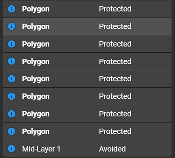
Earlier, Auto‑Layout could inadvertently slice through copper pours—especially smaller ones. Now, any polygon covering less than 10% of the board area is automatically protected from wires and vias unless you explicitly disable that rule.
Auto‑Layout shines when you guide it. Here’s a quick workflow that scales from beginners to power users:
Either way, Auto‑Layout becomes a force multiplier—not a replacement for your expertise.
This Summer Update is a milestone on our roadmap. In the coming months, expect deeper AI understanding of complex topologies, tighter integration with constraint management, and collaborative features that let teams iterate on one layout in real time.
Your feedback is the compass that guides us. Try the Summer Update today—log in, hit “Auto‑Layout”, and tell us where it shined or stumbled via in‑app feedback or our Slack channel. Together, let’s make routing the easiest part of hardware design.


Today, we’re excited to be launching the next step in Copilot’s evolution: the Copilot Context Menu. It lets you access Copilot with the click of a button. Simply right-click on a component or project, and choose the prompt you want to use.


With Flux, enterprises can take their architectural ideas and use AI to transform those ideas into actionable items. With Copilot, your enterprise can generate schematics, perform AI design reviews, and even identify PCB technology, budgets, and timelines well in advance of any manufacturing.

Imagine designing a PCB in a third less time than you're used to - that's the power of Flux Copilot's new upgrade, allowing it to wire components together for you. In this tutorial, we'll walk you through the important workflows and example prompts to help you design a Raspberry-Pi-Pico-like board in 20 minutes.
Creating a manufacturable, error-free PCB is never simple. Every engineer knows that missed details lead to production delays, costly revisions, and project setbacks. But what if you could have the power of a seasoned review team guiding you, 24/7?

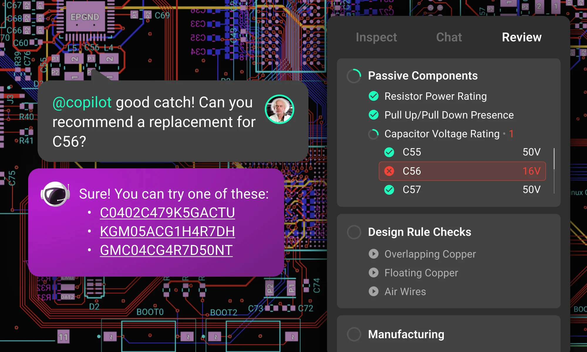
We're excited to reveal a major upgrade - Flux Copilot is transitioning from being a helpful guide to a proactive partner. It no longer just advises but, with your approval, can now wires components together! This is a small step towards fully generative AI, reducing the time and complexity often associated with component connections.
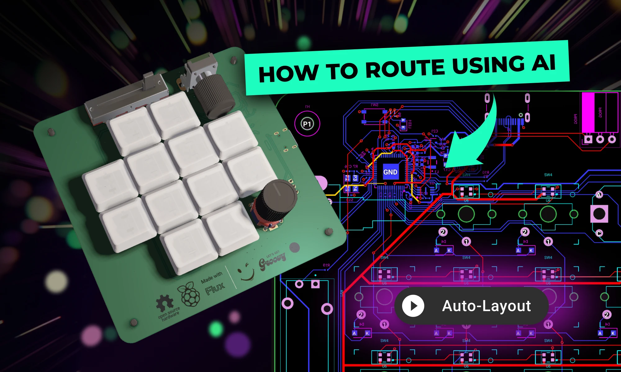
Want to design your own macropad? Discover how to create one using the Raspberry Pi Pico 2 and Flux's AI Auto-Layout. From schematics and components to PCB layout and firmware, we’ve got you covered. Boost your productivity with a custom macropad—start building today!

Flux Copilot helps your team tackle the complexities of PCB cost optimization, identifying hidden savings and providing engineers with actionable insights to streamline design processes and reduce costs.

With Copilot, the brainstorming process is easy. Given your requirements, just prompt Copilot and it will dynamically generate and evaluate architectural variations, balancing technical specifications and regulatory requirements in real time.

Imagine an AI teammate that doesn’t just chat about your PCB ideas, but actively transforms them into schematics—placing parts, connecting circuits, and optimizing your design at your command, all through natural language. That’s exactly what the newly overhauled Flux Copilot does.

Design review is one of the most time-consuming and expensive parts of the hardware design process. Most engineers spend over 30% of their time performing design reviews. What if we could reduce that so that products could ship 30% faster and 30% cheaper?

Integrating AI into hardware development just became easier. Improve your research and planning phase with Flux Copilot—no need to change your existing tools.

Discover how Copilot transforms hardware design from concept to creation through an end-to-end example of designing a webcam, showcasing the power of AI hardware design at every step.